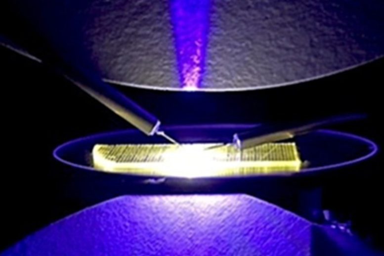
The gallium nitride purple surface-emitting laser with a power conversion efficiency of more than 20%. Credit: Tetsuya Takeuchi / Meijo University
Researchers have created a new technique for precise control of cavity length in GaN-based vertical-cavity surface-emitting lasers.
Gallium nitride (GaN) vertical-cavity surface-emitting lasers (VCSELs) are semiconductor laser diodes with promising applications in various fields, including adaptive headlights, retinal scanning displays, point-of-care testing systems, and high-speed visible light communication systems. Their high efficiency and low manufacturing costs make them especially appealing for these applications.
GaN-VCSELs are composed of two layers of special semiconductor mirrors, called distributed Bragg reflectors (DBRs), separated by active GaN-semiconductor layers, which form the optical resonant cavity, where laser light is generated. The length of this resonant cavity is crucial for controlling the target laser wavelength, called the resonance wavelength.
Development of GaN-VCSEL Structures
Thus far, two types of GaN-based VCSEL structures have been developed: one with a bottom dielectric DBR and the other with bottom aluminum indium nitride (AlInN)/GaN DBR. Both of them result in VSCELs with over 20 milliwatts of light output power and an over 10% wall plug efficiency (WPE). However, the AlInN/GaN DBR has a narrow stop wavelength bandwidth, which allows light only within a narrow wavelength range to be emitted from the VCSELs.
Moreover, the traditional cavity length control method, which involves pre-experiments with test cavity layers for the determination of their growth rate, results in an error between the estimated and final thickness of the VCSEL cavity. This error could lead to resonance wavelengths being out of the narrow stop bandwidth of the AlInN/GaN DBR, significantly affecting performance.
Innovations in Cavity Length Control
To address this issue, in a recent study, researchers from Japan, led by Professor Tetsuya Takeuchi from the Department of Materials Science and Engineering at Meijo University, developed a new in situ cavity length control method for a GaN-based VCSEL optical cavity. By precisely controlling the growth of GaN layers using in situ reflectivity spectra measurements, the researchers achieved precise cavity length control with only a 0.5% deviation from the target resonance wavelength. Now, they have further expanded this innovative technique and demonstrated cavity length control of a complete VSCEL.
Prof. Takeuchi explains, “The cavity of a VCSEL contains not only GaN layers but also an indium tin oxide (ITO) electrode and a niobium pentoxide (Nb2O5) spacer layer, which cannot be controlled with the same in situ reflectivity spectra measurement system. In this study, we developed a technique to precisely calibrate the thickness of these additional layers, resulting in highly efficient VCSELs.” Their study was published in Volume 124, Issue 13 of the journal Applied Physics Letters.
Calibration Techniques for Additional Layers
To calibrate the thickness of the additional layers, the researchers first deposited the ITO electrodes and Nb2O5 spacer layers with varying thicknesses on the GaN test structures that were grown using the in situ cavity control. Given that the in situ reflectivity measurement cannot be used for these additional layers, they directly evaluated the resonance wavelength of these test cavity structures using ex situ reflectivity spectra measurement. The obtained resonance wavelengths were redshifted, meaning the wavelengths were increased with an increase in the thickness of ITO and Nb2O5 layers.
Next, the researchers mapped the resonance wavelength shifts as a function of the ITO and Nb2O5 layer thicknesses, obtaining accurate information about their optical thicknesses. They used this information to precisely calibrate the thickness of the ITO and Nb2O5 layers towards the target VCSEL resonance wavelength. The deviation of resonance wavelength control resulting from this method was sufficiently low, within 3%, comparable to the in situ control method in terms of optical thickness.
Finally, the researchers fabricated GaN-VCSELs with aperture sizes ranging from 5 to 20 µm by implementing the tuned ITO electrodes and Nb2O5 spacer layers into the VCSEL cavity grown using the in situ cavity control. The peak emission wavelength of these VCSELs had a deviation of merely 0.1% from the designed resonance wavelength. Notably, thanks to the precise cavity length control, the 5-µm aperture VCSEL achieved a WPE of 21.1%, marking a significant achievement.
“Just like a highly accurate scale enables the construction of detailed shelves, the precise use of in situ thickness control of GaN layers combined with thickness calibration of ITO electrodes and Nb2O5 spacer layers enables highly controlled fabrication of VCSELs, representing a powerful tool for obtaining high-performance and highly reproducible GaN-based VCSELs for highly efficient optoelectronic devices,” concludes Prof. Takeuchi, highlighting the importance of these findings.
Reference: “Over 20% wall plug efficiency of on-wafer GaN-based vertical-cavity surface-emitting laser” by Ruka Watanabe, Kenta Kobayashi, Mitsuki Yanagawa, Tetsuya Takeuchi, Satoshi Kamiyama, Motoaki Iwaya and Toshihiro Kamei, 28 March 2024, Applied Physics Letters.
DOI: 10.1063/5.0200294
>>> Read full article>>>
Copyright for syndicated content belongs to the linked Source : SciTechDaily – https://scitechdaily.com/gan-vcsels-hit-new-milestones-japanese-researchers-achieve-unprecedented-resonance-control/