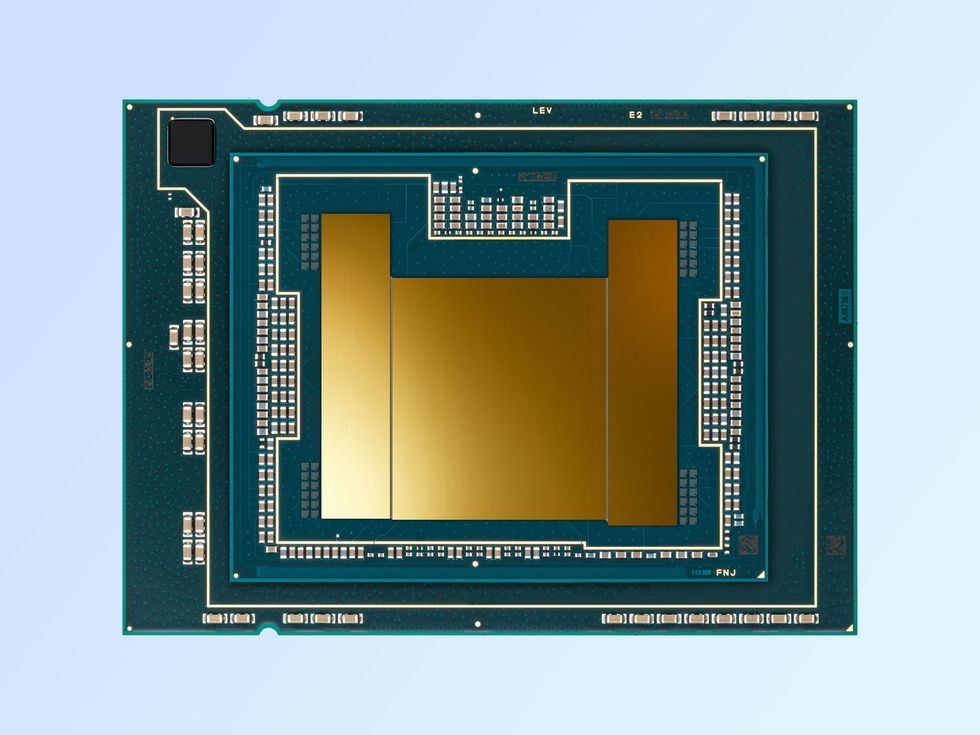
Last week at VLSI Symposium, Intel detailed the manufacturing process that will form the foundation of its foundry service for high-performance data center customers. For the same power consumption, the Intel 3 process results in an 18 percent performance gain over the previous process, Intel 4. On the company’s roadmap, Intel 3 is the last to use the fin field-effect transistor (FinFET) structure, which the company pioneered in 2011. But it also includes Intel’s first use of a technology that is essential to its plans long after the FinFET is no longer cutting edge. What’s more, the technology is crucial to the company’s plans to become a foundry and make high-performance chips for other companies.
Called dipole work-function metal, it allows a chip designer to select transistors of several different threshold voltages. Threshold voltage is the level at which a device switches on or off. With the Intel 3 process, a single chip can include devices having any of four tightly-controlled threshold voltages. That’s important because different functions operate best with different threshold voltages. Cache memory, for example, typically demands devices with a high threshold voltage to prevent current leakage that wastes power. While other circuits might need the fastest switching devices, with the lowest threshold voltage.
Threshold voltage is set by the transistor’s gate stack, the layer of metal and insulation that controls the flow of current through the transistor. Historically, “the thickness of the metals determines the threshold voltage,” explains Walid Hafez, vice president of foundry technology development at Intel. “The thicker that work function metal is, the lower the threshold voltage is.” But this dependence on transistor geometry comes with some drawbacks as devices and circuits scale down.
Small deviations in the manufacturing process can alter the volume of the metal in the gate, leading to a somewhat broad range of threshold voltages. And that’s where the Intel 3 process exemplifies the change from Intel making chips only for itself to running as a foundry.
“The way an external foundry operates is very different” from an integrated device manufacturer like Intel was until recently, says Hafez. Foundry customers “need different things… One of those things they need is very tight variation of threshold voltage.”
Intel is different; even without the tight threshold voltage tolerances, it can sell all its parts by steering the best performing ones toward its datacenter business and the lower-performing ones in other market segments.
“A lot of external customers don’t do that,” he says. If a chip doesn’t meet their constraints, they may have to chuck it. “So for Intel 3 to be successful in the foundry space, it has to have those very tight variations.”
Dipoles ever after
Dipole work function materials guarantee the needed control over threshold voltage without worrying about how much room you have in the gate. It’s a proprietary mix of metals and other materials that, despite being only angstroms thick, has a powerful effect on a transistor’s silicon channel.
Like the old, thick metal gate, the new mix of materials electrostatically alters the silicon’s band structure to shift the threshold voltage. But it does so by inducing a dipole—a separation of charge—in the thin insulation between it and the silicon.
Because foundry customers were demanding tight control of Intel, it’s likely that competitors TSMC and Samsung already use dipoles in their latest FinFET processes. What exactly such structures are made of is a trade secret, but lanthanum is a component in earlier research, and it was the key ingredient in other research presented by the Belgium-based microelectronics research center, Imec. That research was concerned with how best to build the material around stacks of horizontal silicon ribbons instead of one or two vertical fins.
In these devices, called nanosheets or gate all-around transistors, there are mere nanometers between each ribbon of silicon, so dipoles are a necessity. Samsung has already introduced a nanosheet process, and Intel’s, called 20A, is scheduled for later this year. Introducing dipole work function at Intel 3 helps get 20A and its successor 18A into a more mature state, says Hafez.
Flavors of Intel 3
Dipole work-function was not the only technology behind the 18 percent boost Intel 3 delivers over its predecessor. Among them are more perfectly formed fins, more sharply defined contacts to the transistor, and lower resistance and capacitance in the interconnects. (Hafez details all that here.)
Intel is using the process to build its Xeon 6 CPUs. And the company plans to offer customers three variations on the technology, including one, 3-PT, with 9-micrometer through-silicon-vias for use in 3D stacking. “We expect Intel 3-PT to be the backbone of our foundry processes for some time to come,” says Hafez.
>>> Read full article>>>
Copyright for syndicated content belongs to the linked Source : IEEE – https://spectrum.ieee.org/intel-foundry-finfet
