Home » Artificial intelligence » Ultraviolet Metalenses Mass Produced. Will Enable Future AI Chips
Extreme Ultraviolet lithography for computer chips have been critical to letting us efficiently get better than 14 nanometer computer chips. Metalenses are 10,000 times thinner than regular lenses.
Metalenses control light properties through nanometer-scale patterns or structures on lens surfaces. With the ability to reduce the thickness of conventional lenses by a factor of 10,000, they hold significant promise in medical devices that are inserted in the body and wearable devices. Ongoing active research aims to achieve mass production and commercialization of metalenses.
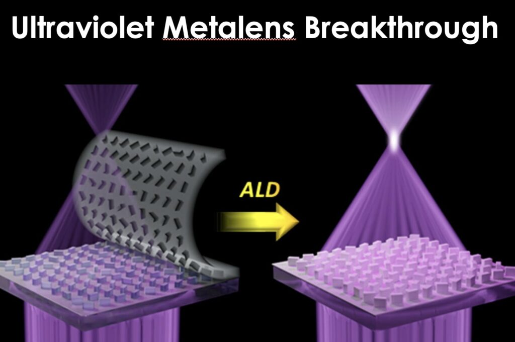
Researchers have devised a technique for the mass production of large-area metalenses tailored for use in the ultraviolet region.
Ultraviolet light poses challenges as it is absorbed by most materials due to its high energy level.
The team used a nano-imprinting process that engraves the pattern like a stamp. They achieved the rapid and inexpensive production of metalenses that are 20,000 times larger than conventional ones.
Metalenses have outstanding light-modulating performances, and studies have been conducted on them to not only replace conventional bulky and heavy refractive lenses but also to expand on them. However, their operating wavelengths have rarely covered the ultraviolet (UV) regime since UV-transparent materials are scarce and nanopatterning techniques have a small patterning area, high cost, and low throughput.
These limitations are overcome in this study, and centimeter-scale and highly efficient UV metalenses are successfully mass-produced. The UV metalens is designed to operate at a wavelength of 325 nm, with a numerical aperture of 0.2. Argon fluoride photolithography is used to fabricate an 8-inch master stamp in which 300 metalenses are patterned in an array with a high resolution. The fabricated master stamp can be duplicated repeatedly using wafer-scale nanoimprint lithography. To improve efficiency, we developed a zirconium dioxide–polymer hybrid material that is scalable, easily manufacturable, UV-transparent, and high-index material. The experimental results confirm that the mass-produced metalenses operate as ideal imaging systems, exhibiting an average measured efficiency of 45.1 %.
Brian Wang is a Futurist Thought Leader and a popular Science blogger with 1 million readers per month. His blog Nextbigfuture.com is ranked #1 Science News Blog. It covers many disruptive technology and trends including Space, Robotics, Artificial Intelligence, Medicine, Anti-aging Biotechnology, and Nanotechnology.
Known for identifying cutting edge technologies, he is currently a Co-Founder of a startup and fundraiser for high potential early-stage companies. He is the Head of Research for Allocations for deep technology investments and an Angel Investor at Space Angels.
A frequent speaker at corporations, he has been a TEDx speaker, a Singularity University speaker and guest at numerous interviews for radio and podcasts. He is open to public speaking and advising engagements.
>>> Read full article>>>
Copyright for syndicated content belongs to the linked Source : Next Big Future – https://www.nextbigfuture.com/2024/03/ultraviolet-metalenses-mass-produced-will-enable-future-ai-chips.html
