TechSpot is celebrating its 25th anniversary. TechSpot means tech analysis and advice you can trust.
Forward-looking: Canon is renowned for its printers, cameras, and other imaging products designed for both consumer and industrial use. The Japanese company is now applying its extensive knowledge in optical and imaging technologies to venture into the highly specialized field of advanced chip manufacturing equipment.
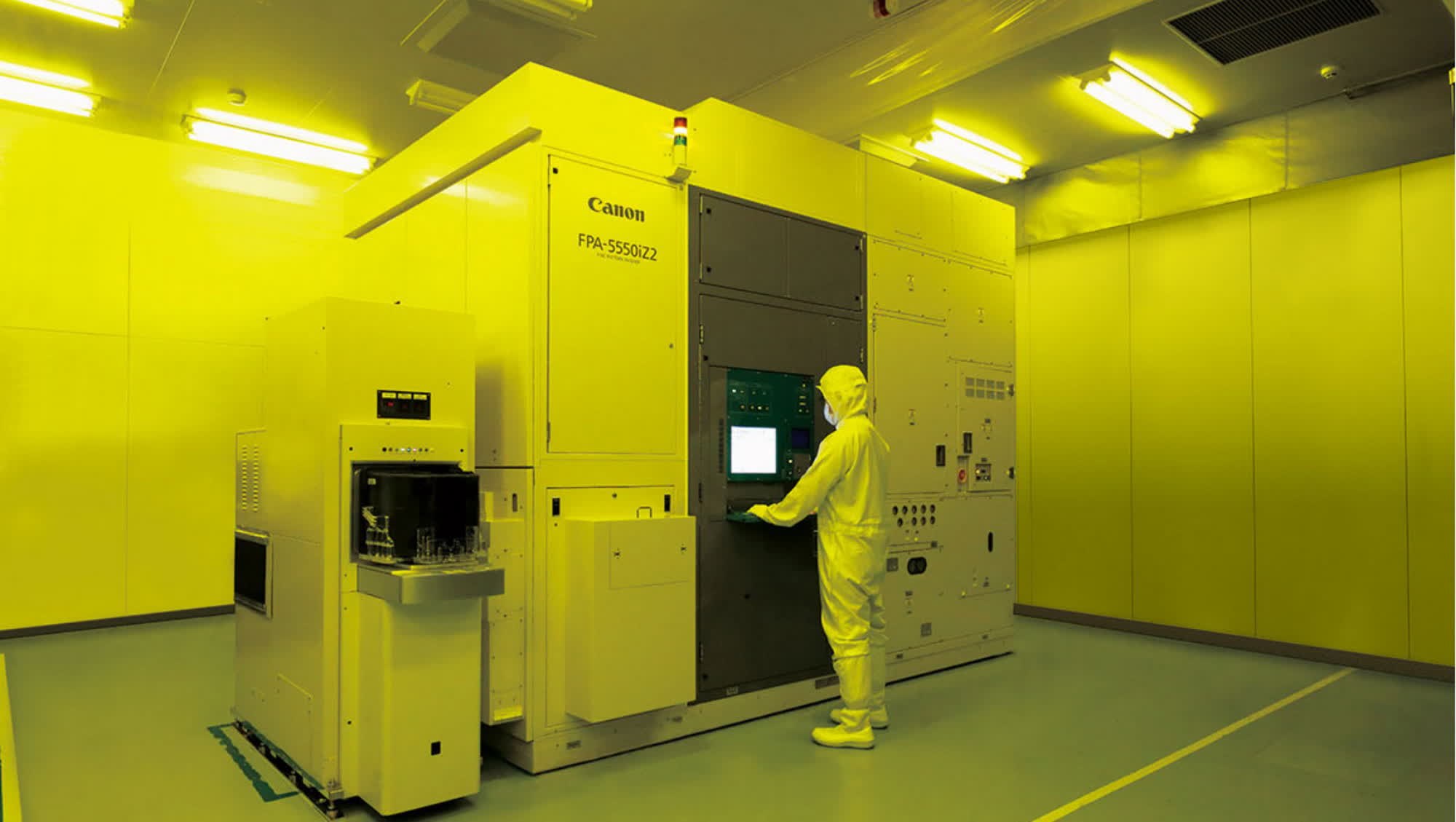
Canon recently introduced the FPA-1200NZ2C, a piece of “nanoimprint semiconductor manufacturing” equipment specifically designed for producing microchips and other semiconductor-based components using the latest manufacturing nodes available. Canon’s solution for chip manufacturing appears to offer similar capabilities to its competitors but does so with significantly lower power consumption, thanks to its utilization of nanoimprint technology.
Unlike traditional photolithography systems, nanoimprint lithography (NIL) does not rely on an optical mechanism to transfer a circuit pattern onto the resist-coated wafer. Canon’s NIL machinery achieves the same outcome by pressing a mask imprinted with the circuit pattern onto the wafer’s resist, essentially acting like a stamp, as described by the company.
The FPA-1200NZ2C can handle patterning workloads with a minimum linewidth of 14 nm, a capability that Canon states is comparable to the 5nm manufacturing node necessary for producing today’s “most advanced logic semiconductors.” Canon anticipates that, with continued enhancements in mask technology, the NIL technique is poised to reach a minimum linewidth of 10 nm (equivalent to a 2nm node).

The new FPA-1200NZ2C device is also equipped with innovative environmental control technology designed to minimize fine particle contamination. Since it doesn’t require a “special” light source like extreme ultraviolet (EUV) lithography machines, Canon’s NIL solution is notably energy-efficient and can significantly reduce power consumption, thereby contributing to CO2 reduction.
The FPA-1200NZ2C is capable of manufacturing complex semiconductor circuits with an increasing number of defect-free layers, thanks to the aforementioned fine particle control technology. Canon states that this machinery can be utilized for a wide range of applications, including metalenses for extended reality (XR) devices with microstructures in the tens of nanometers, as well as logic circuits in CPUs and various other semiconductor devices.
Nanoimprint lithography is a technique that has been in existence for over 20 years, as noted by Pranay Kotasthane, the chairperson of the Takshashila Institution, in an interview with CNBC. However, the technology failed to gain significant traction, primarily because extreme ultraviolet (EUV) machines produced by the Dutch company ASML delivered superior results for highly sophisticated chip products. Canon, which has been developing its NIL technology since 2004, is now banking on the idea that this “cheaper” solution is “good enough” for producing advanced microchips independently.
>>> Read full article>>>
Copyright for syndicated content belongs to the linked Source : TechSpot – https://www.techspot.com/news/100489-canon-challenges-asml-supremacy-chip-manufacturing-new-nanoimprint.html


